SFQ pulse generator¶
At a glance¶
| Property | Value |
|---|---|
| Project name | SFQ-generator |
| Version | v1 |
| Function | SFQ pulse generator testbench |
| Subcircuits instantiated | DCSFQ ×1, JTL ×2 (JTL1, JTL2) |
| Josephson junctions | 7 (3 in DCSFQ, 2 in each JTL) |
| Junction models used | JJ225 ×2, JJ250 ×5 |
| Stimulus sources | 2 (IPULSE1, IPULSE2) |
| Internal bias sources | 4 (IPWL1/IPWL2 in DCSFQ; IPWL1 in each JTL) |
| Inductors | 20 (8 in DCSFQ, 6 in each JTL) |
| Damping/output resistors | 8 (3 in DCSFQ, 2 in each JTL, Rout) |
| Total device count | 41 |
| Ports | none (self-contained testbench; output taken across Rout) |
| Transient analysis window | 0–400 ps, 0.5 ps step (TRAN1) |
| Simulators supported | JSIM, JoSIM |
Function¶
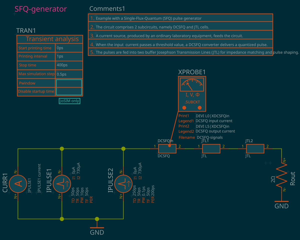
This testbench feeds a current-pulse stimulus into a DCSFQ cell, which converts the transition into a train of quantized Single Flux Quantum (SFQ) voltage pulses. The input pulses are typically produced by ordinary laboratory equipment, so their width does not need to be short — in fact it should never be shorter than the circuit's characteristic time, typically a few ps. The DCSFQ cell converts a low-frequency input signal (loosely called "DC") into SFQ pulses by acting like a Schmitt-trigger: it produces one quantized pulse (area ≈ 2.07 mV·ps) each time the rising input current crosses a threshold. See detailed explanation of the DCSFQ cell in the Appendix.
The pulses are then propagated through two cascaded JTL (Josephson Transmission Line) cells for impedance matching and pulse reshaping before reaching the output termination Rout. See JTL cell explanation here.
Signal path: stimulus → DCSFQin (DCSFQ cell) → JTL2 → JTL1 → Rout/GND.
Expected results¶
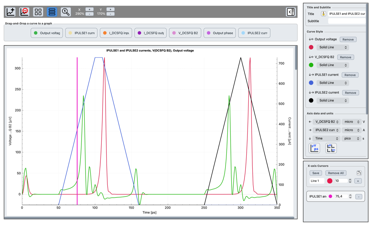
Two ammeters have been placed on the circuitry to monitor two parallel sources of current pulses. Their parameters can be modified to see the influence of the pulse width, rise and fall times, as well as the period. Note that JSIM and JoSIM simulators have a slightly different interpretation of the period (see §5.2 of the SuperLibre library reference file). The output voltage is superposed with the two current input sources in the following figure.One can notice that the output voltage pulses (in red) are triggered after the input currents reach their maximum This is in fact misleading since the pulses take some time to propagate from the input to the output of 3 cells (DCSFQ + 2 JTLs). In fact the first junction that is triggered is B2 from the DCSFQ cell (green curve) at about t=75ps when the input current reaches 150µA.
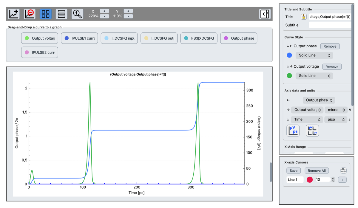
The next figure shows a superposition of the output voltage and phase, showing clearly how the voltage pulses are a marker of phase changes. However the different states of the circuit are identified by the phase. The voltage, being the derivative, loses the information about the phase and the energy of the circuit.
Bias¶
| Source | Feeds | Current / waveform | Role |
|---|---|---|---|
| IPULSE1 | DCSFQ input node | 0 → 730 µA pulse (delay 50 ps, width 10 ps) | Single trigger pulse — crosses the DCSFQ threshold |
| IPULSE2 | DCSFQ input node | 0 → 730 µA pulse train (delay 250 ps, width 0.1 ps, period 200 ps) | Periodic stimulus for repeated SFQ generation |
| IPWL1 / IPWL2 (DCSFQ) | internal DCSFQ nodes | 275 µA / 175 µA | Bias the DCSFQ input/output stages |
| IPWL1 (JTL1, JTL2) | internal JTL nodes | 350 µA each | Bias each JTL buffer stage |
IPULSE1 and IPULSE2 are both wired to the same input node in this example; only one stimulus profile is normally active at a time depending on which excitation is being exercised.
Junction models used¶
| Parameter | JJ225 | JJ250 |
|---|---|---|
| ICRIT | 225 µA | 250 µA |
| RN | 90 Ω | 90 Ω |
| R0 | 130 Ω | 130 Ω |
| CAP | 1.125 pF | 1.25 pF |
| VG | 2.85 mV | 2.85 mV |
| DELV | 0.01 mV | 0.01 mV |
| T | 4.2 K | 4.2 K |
| TC | 9.26 K | 9.26 K |
| Used by | DCSFQ (B1, B2) | DCSFQ (B3); JTL1/JTL2 (B1, B2 each) |
Separate parameter sets are defined for JSIM and JoSIM, since the two simulators expect slightly different model syntax.
Copyright (C) 2025-2026 SEFIRA. Licensed under the Apache 2.0 license.