Appendix: Detailed explanation of the DCSFQ cell
BACK to the explanation of the SFQ GENERATOR circuit
At a glance
| Property | Value |
|---|---|
| Cell name | DCSFQ |
| Function | Converts a low-frequency ("DC") input current into quantized SFQ voltage pulses — one pulse (area ≈ 2.07 mV·ps) per rising threshold crossing |
| Josephson junctions | 3 (B1, B2, B3) |
| Junction models used | JJ225 ×2 (B1, B2), JJ250 ×1 (B3); JJ200 also defined but not instantiated |
| Internal bias sources | 2 (IPWL1, IPWL2) |
| Inductors | 8 (L0, L1, L2, L3, L4, L5 on the signal path; L2p, L3p parasitic) |
| Damping/output resistors | 3 (RB1, RB2, RB3) |
| Total device count | 16 |
| Ports | 2 (INPUT = port 1, OUTPUT = port 2) |
| Josephson inductances | LJ0(B1, B2) ≈ 1.46 pH, LJ0(B3) ≈ 1.32 pH |
| Simulators supported | JSIM, JoSIM |
The DCSFQ cell and its equivalent inductor network are shown below.
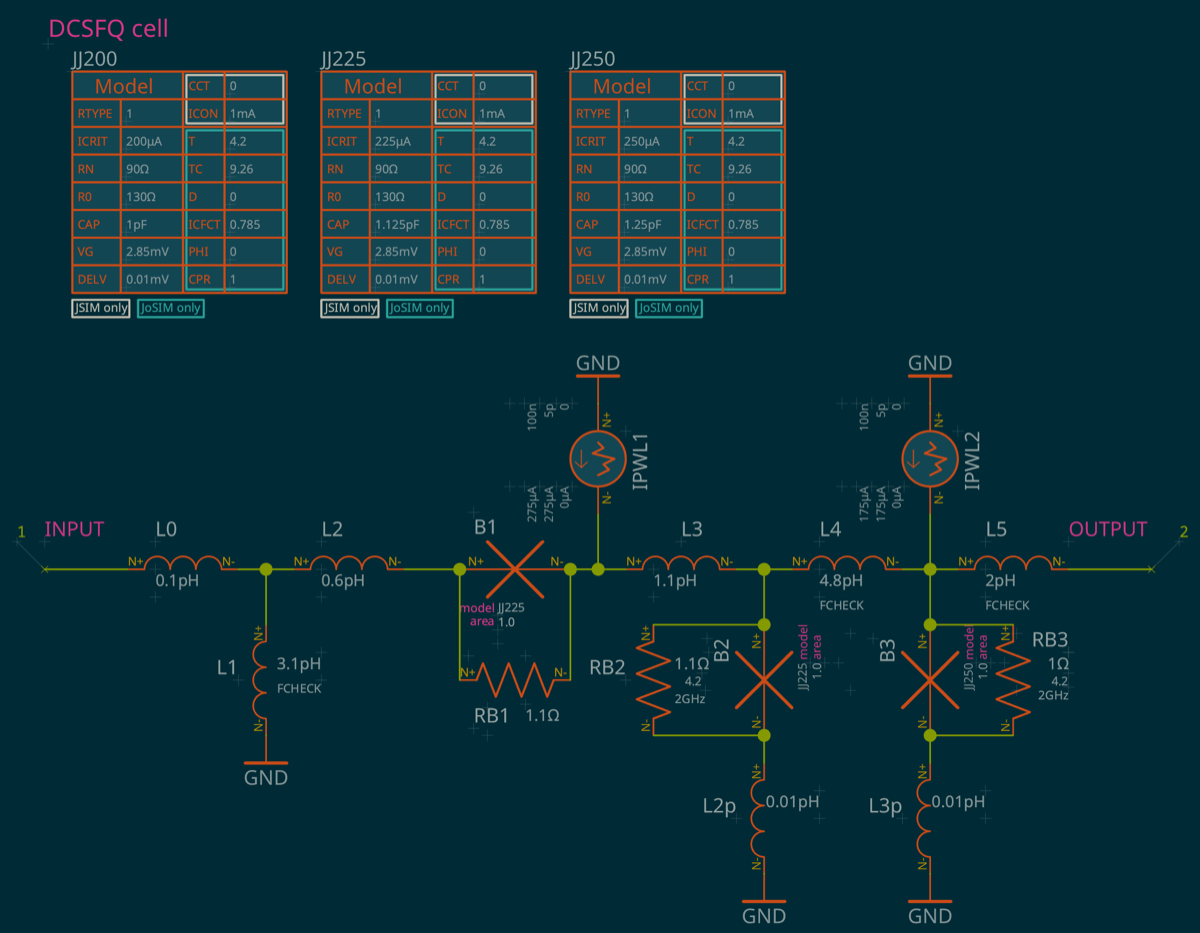
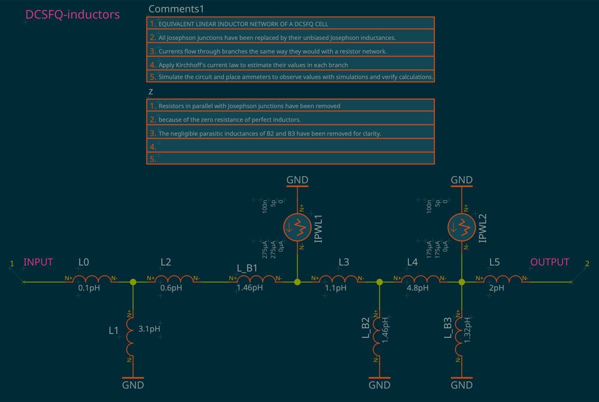
The DCSFQ cell converts an incoming DC current step into a quantized Single Flux Quantum (SFQ) voltage pulse. To understand intuitively how the circuit works, it helps to consider the intrinsic inductive behavior of a Josephson junction (JJ) to first order, without accounting for its non-linear properties.
The equivalent inductance of any unbiased junction is called the Josephson inductance, LJ0 = Φ₀ / (2π·IC). IC is the junction's critical current, while Φ₀ = h/2e = 2.07 mV·ps = 2.07 pH·mA is the quantum of magnetic flux. Here, for instance, LJ0 = 1.46 pH for B1 and B2, and LJ0 = 1.32 pH for B3.
The schematic screenshot above shows the equivalent inductor network obtained once the Josephson junctions are replaced by their unbiased Josephson inductances. The resistors in parallel with the JJs have been removed since they play no role: no current flows through them because of the parallel zero-resistance inductive path.
The first bias current IPWL1 = 275 µA of the DCSFQ cell splits into two parts:
- the path going back towards the input, of inductance LJ0(B1) + L2 + L1 ≈ 5.16 pH (almost no current flows back to the input through L0 because of the very high input inductance due to the long wiring leads on the chip and towards the laboratory equipment);
- the L3 + B2 // [L4 + (B3 // (L5 + Lout))] output path, whose total inductance is about 2.22 pH (see below).
Since DC currents spread through a network of perfect (non-resistive) inductors in the same way they would spread through resistors, Kirchhoff's current law can be generalized.
The maximum current flowing through L4 (coming from L3) is obtained if L4's output is shorted, corresponding to a minimum current in B2 given by LJ0(B2) × I(B2) ≈ L4 × I(L4), since B2 and L4 are in parallel. This leads to I(B2) > 77% of I(L3), the remaining 23% of I(L3) flowing through L4 and B3. In other words, the incoming IPWL1 bias current flowing through L3 goes mostly through the B2 junction.
The minimum equivalent inductance of the output path is consequently L3 + LJ0(B2) // L4 ≈ 1.1 pH + (1.46 pH // 4.8 pH) = 2.22 pH.
Similarly, the IPWL1 current splits unevenly between the input path (through L2, with a total inductance of 5.16 pH) and the output path (through L3, with a total inductance of 2.22 pH): I(L3) = 70% × IPWL1, leading to a minimum current in B2 given by 77% × 70% × IPWL1 = 54% × IPWL1: I(B2)min = 150 µA, a substantial part (67%) of its critical current of 225 µA. The B2 junction is not far from its switching threshold. On the other hand, the B3 junction receives at most 23% × 70% × IPWL1 = 44 µA, corresponding to 18% of its critical current of 250 µA.
Regarding the left branch of B1, of 5.16 pH inductance, the same reasoning leads to a bias current I(B1) = 83 µA. As a result, if the current brought by the input signal is large enough, only B2 will switch and generate a pulse. Indeed, the input signal current brought through B1 flows opposite to the IPWL1 bias current and "de-biases" B1, preventing it from switching. B1 is called an escape junction: it prevents a backward pulse coming from the output from reaching the input. The current of such a backward pulse adds to the bias current of B1; the sum then exceeds B1's critical current and causes it to switch, blocking the backward pulse before it reaches the input.
Once B2 has switched, the incoming input signal pulse is transformed into a single flux quantum Φ₀ that flows clockwise through the B2-L4-B3 loop. The current Ipulse is such that Φ₀ = (LJ0(B2) + LJ0(B3) + L4) × Ipulse, resulting in Ipulse = 273 µA. This current of 273 µA is subtracted from the bias current of B2, reverse-biasing it and preventing B2 from switching again. Conversely, it adds to the 44 µA bias current of B3, causing it to switch immediately and release the flux stored in the loop. Consequently, no flux remains stored in any DCSFQ loop, and a pulse is generated at the output.
This analysis overlooked the second bias current, IPWL2. In fact, some DCSFQ cells don't use it and instead adjust other parameters for optimal cell performance, depending on the desired operating margins. We can, however, explain its role qualitatively here, and we encourage you to change parameters and run simulations to observe the impact of each one in the DCSFQ inductor network example. IPWL2 primarily biases both B2 and B3, with a slight current also flowing to the output. This output current should be kept low to prevent a redistribution of currents once the DCSFQ cell is connected to another cell. Since L4 has a relatively high inductance, most of the IPWL2 current (approximately 80%) flows through B3. This facilitates the switching of B3 once B2 has already switched. In addition, B2 is slightly more biased than the value obtained above from IPWL1 alone, which further aids the switching of B2 in the presence of an incoming pulse.
To summarize, IPWL2 provides finer control over the B3 switching, while IPWL1 manages B2 switching. As a result, the DCSFQ cell's switching tolerance is improved, enabling it to switch as expected across a wider range of circuit parameter values. It also helps decouple the two junctions, leading to cleaner output pulses. Each junction switching is accompanied by sharp current and voltage changes in the circuit, which can be "sensed" by neighboring junctions and disturb their own behavior. The B2 pulse is affected by B1 "shaking" even when B1 does not switch; B3 then reshapes the fluxon emitted by B2 into a clean output pulse.
The DCSFQ output pulses are then propagated through two cascaded JTL (Josephson Transmission Line) cells for impedance matching and pulse reshaping before reaching the output termination Rout. See JTL cell explanation here.
Bias
| Source | Feeds | Current / waveform | Role |
|---|---|---|---|
| IPWL1 | B1–L3 node (top of B2) | PWL 0 → 275 µA (rise over 0–5 ps, held to 100 ns) | Primary bias — sets B2 just below its switching threshold |
| IPWL2 | L4–L5 node (top of B3) | PWL 0 → 175 µA (rise over 0–5 ps, held to 100 ns) | Secondary bias — biases B2 and B3, sharpens B3 switching and decouples the two junctions |
Both sources are piecewise-linear current sources: current ramps from 0 to its final value between t = 0 and t = 5 ps, then stays constant up to 100 ns.
Junction models used
| Parameter | JJ200 | JJ225 | JJ250 |
|---|---|---|---|
| ICRIT | 200 µA | 225 µA | 250 µA |
| RN | 90 Ω | 90 Ω | 90 Ω |
| R0 | 130 Ω | 130 Ω | 130 Ω |
| CAP | 1.0 pF | 1.125 pF | 1.25 pF |
| VG | 2.85 mV | 2.85 mV | 2.85 mV |
| DELV | 0.01 mV | 0.01 mV | 0.01 mV |
| T | 4.2 K | 4.2 K | 4.2 K |
| TC | 9.26 K | 9.26 K | 9.26 K |
| Used by | — (defined, not instantiated) | B1, B2 | B3 |
Each model also carries simulator-specific fields — CCT, RTYPE, ICON for JSIM and ICFCT, PHI, CPR, D for JoSIM — since the two simulators expect slightly different model syntax.
BACK to the explanation of the SFQ GENERATOR circuit
Copyright (C) 2025-2026 SEFIRA. Licensed under the Apache 2.0 license.